Onboard chargers

(Image courtesy of Nissan)
Charging ahead
Nick Flaherty examines how designers are making OBCs more powerful, faster and lighter
The onboard charger (OBC) market is changing with increasing power levels for faster operation and the need for lighter systems that can be integrated with the other vehicle components.
OBCs convert alternating current (AC) from the grid into direct current (DC) that can be stored in the vehicle’s 400 V, or now 800 V, battery. Their efficiency and reliability have an impact on the overall performance and user experience of the vehicle, making them a key focus area for EV manufacturers.
This move to battery packs of 800 V (or even higher) is driving the need for greater power and more efficient OBCs.
Designers are looking at integrating the OBC with low-voltage DC-DC converters, which is critical to convert high-voltage power (400 V or 800 V) to low voltage (12 V or 48 V) efficiently, along with support for different AC inputs (single- or three-phase). All this is driving innovation in design with various topologies for both the charger and the power suppliers for the various components in the charger.
Battery performance and durability are also highly dependent on the charging technologies and methods.
Thermal management is also critical to ensure proper operation and longevity of OBC systems, especially at higher power levels. So, these systems must comply with relevant safety standards and regulations governing EV charging infrastructure, such as IEC 61851 and SAE J1772, and they should support communication interfaces for seamless integration with the vehicle’s onboard network and external charging framework.
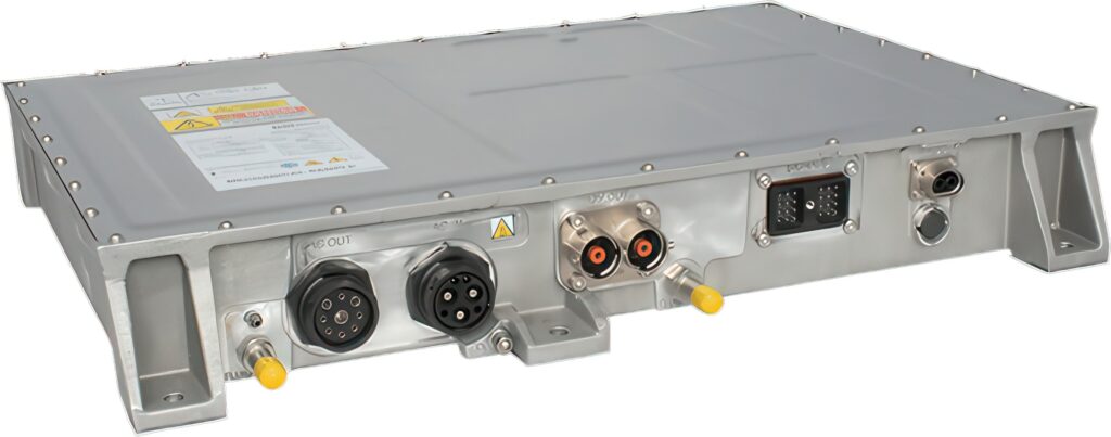
(Image courtesy of Bel Power)
OBC topologies
The latest battery-electric vehicles deploy battery capacities up to approximately 100 kWh, which allows Worldwide Harmonised Light Vehicle Test Procedure (WLTP) ranges over 400 km. Vehicle designs with even higher capacities have been in development to accelerate the maximum achievable range possible with a single charge.
The OBCs in consumer vehicles typically support power ratings to 22 kW, as found in charging parks, besides lower-power 3.3 kW and 11 kW chargers in the home. DC fast charging with power ratings up to 400 kW is a separate DC-DC circuit that can be integrated alongside the OBC.
An OBC typically offers a unidirectional power flow from the grid to the battery, although there is increasing focus on bidirectional charging and connectivity for the European and US markets.
Charging via the main grid calls for design flexibility due to the varying voltage and current levels in different countries. System designers face the challenge of supporting these variables while increasing power density.
In the case of AC charging, an OBC is handling the conversion of AC power into the DC power required by the battery.
The power losses during conversion subtract from the power available to charge, so the efficiency of the conversion from AC to DC is key.
Today’s OBCs are typically targeting 95% of total AC-DC efficiency or above, which reduces losses and means less heat is generated in the system, so less effort needs to be spent on thermal management.
This is also key for shrinking the size of the OBC, as the heat sink or liquid cooling system can be smaller, and integrated with the DC-DC converter with shared cooling. This boosts overall power density.
Another requirement for OBC systems is for them to be scalable, and hence able to deal with the various power classes and AC inputs all over the world.
The OBC topology consists of a power-factor correction (PFC) stage, the DC link and a DC-DC block.
An important requirement for the OBC system is to achieve high efficiency in the conversion by minimising power losses. The advantage of the power loss reduction is twofold: a higher efficiency delivers more energy to the battery and thus the charging process is faster; secondly, higher efficiency means lower power losses.
Several technologies are suitable for the AC-DC conversion, from silicon IGBTs, silicon and silicon carbide (SiC) MOSFET transistors to gallium nitride (GaN) transistors.
The majority of OBCs are galvanically isolated AC-DC converters, offering modularity on the power classes and interoperability with different AC grids.
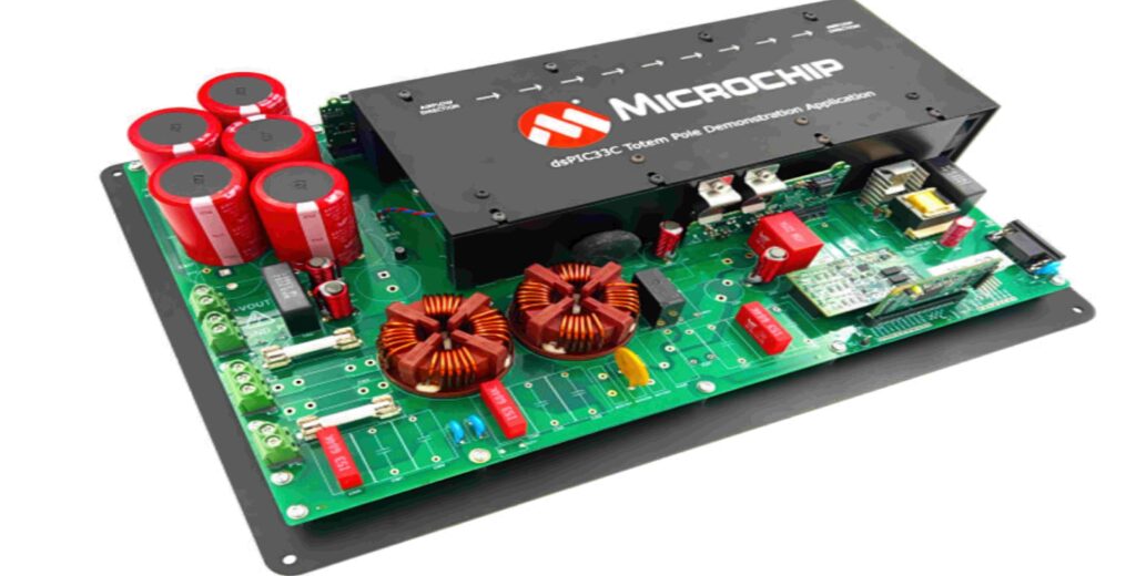
(Image courtesy of Microchip)
Power factor correction
Many PFC topologies are used in the industry, from a classical boost topology to a dual boost or even a totem-pole design.
The vast majority of PFC stages in OBCs are being operated in continuous current mode (CCM), which leads to the requirement of semiconductors that are robust against hard commutation on their body diode. Superjunction silicon MOSFETs can be used in CCM PFC stages with a silicon-carbide diode as the commutation partner.
An alternative is to use SiC wide-bandgap MOSFETs in a CCM PFC as these technologies are inherently robust against hard commutation. In this case, two switches can be used in a half-bridge configuration, whereas the superjunction MOSFET works in combination with a SiC diode.

(a) IGBT with integrated SiC diode; (b) single IGBT with external protection diode; and
(c) CoolMOS CFD7A (with intrinsic body diode)
(Image courtesy of Infineon Technologies)
Classical boost PFC
The simplest topology to achieve a power-factor-correction functionality is to use a simple boost-converter topology, known as ‘classic PFC’ or ‘classic boost PFC’.
This simple circuit comprises a half-bridge configuration with a switch and a diode, an inductor, and a diode bridge rectifier on the AC input side. On the DC output side, buffer capacitors are commonly used to stabilise the output voltage. The most common mode of operation to achieve a high power factor is CCM, achieved by the hard commutation of the current between the switch and the diode. This topology offers a unidirectional power flow from the AC input to the DC output.
Various semiconductor switches can be used as a power switch in the PFC stage. IGBTs are available as single IGBTs, or IGBTs with an integrated silicon or SiC diode. If single IGBTs are used, a small, anti-parallel PN diode between the collector and emitter nodes avoids negative voltage spikes.
However, using a MOSFET instead of an IGBT provides higher efficiency conversion as it has a resistive behaviour in the channel, does not suffer from a tail current, and offers lower switching losses over temperature compared with an IGBT. All this leads to lower power losses and higher conversion efficiency.
Another possibility is to use a wide-bandgap MOSFET or GaN transistor in the classic boost PFC. Nonetheless, the efficiency would not increase since the former cannot fully exploit the advantages of its wide-bandgap material in this topology.
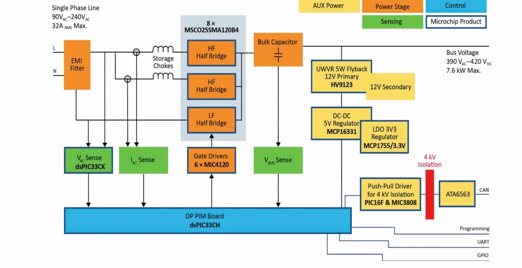
(Image courtesy of Microchip)
Dual-boost PFC
An alternative topology for a unidirectional OBC is a ‘bridgeless’ PFC design, which does not use a diode bridge on the AC input side. Instead, it uses semiconductor switches to increase efficiency.
The working principle of the dual-boost topology is very similar to the classic boost PFC, but each AC semi-cycle is handled by one dedicated half-bridge instead of rectifying the AC. This raises the number of active switches, but also increases conversion efficiency due to the absence of the diode rectifier on the input.

(Image courtesy of Infineon Technologies)
Totem-pole PFC
A common topology for bidirectional OBCs is the totem-pole PFC, where all the diodes are replaced with active power switches, boosting efficiency. Although this is more complex in terms of the components and control algorithms, requiring a more sophisticated controller, the performance of cost-effective controllers is increasing with several automotive-qualified parts available with optimised switching algorithms.
The totem-pole PFC consists of a fast-switching leg and a slow-switching leg. The fast one requires semiconductors that can withstand hard commutation of the load current in between two active switches at high frequency.
The switches in the slow-switching leg are fulfilling a phase rectification functionality. Thus, they are turned on and off with the AC frequency of 50 Hz or 60 Hz during zero crossings of the AC input (zero voltage switching, or ZVS).
Silicon superjunction MOSFETs can be used in the phase rectification leg due to the soft-switching at AC frequency.
With ultra-low, reverse recovery charge, SiC MOSFETs can be used for a hard-switching, totem-pole PFC, comprising four SiC MOSFETs with a 1200 V breakdown voltage. This enables support for higher DC link voltages (above 650 V).
Soft-switching also enables the use of MOSFETs in full-bridge topologies. These PFC stages are commonly known as ‘triangular current mode’ PFCs. The disadvantage of this approach is that a variable frequency is required to control the stages and the power factor decreases in comparison with a CCM PFC. This could be compensated for by an interleaving of several soft-switching PFC stages.
The DC-DC converter stage in an OBC is an isolated DC-DC block to provide the requirements in terms of isolation and safety. Furthermore, this stage plays a role in regulating the actual charging voltage on its output, depending on the state of the high-voltage traction battery.
The most common topologies are soft-switching, phase-shifted, full-bridge converters and LLC converters. Due to the superior switching speed, MOSFETs play a dominant role in modern DC-DC converters.
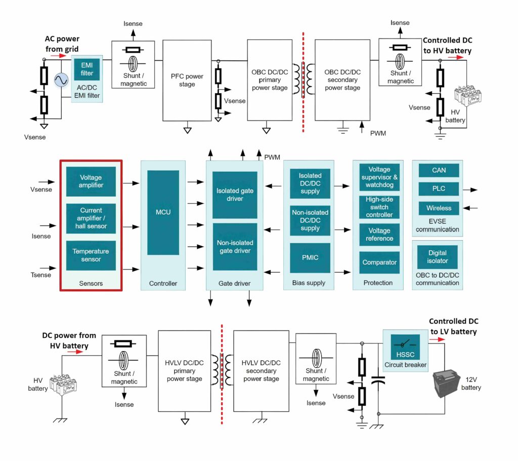
(Image courtesy of Texas Instruments)
Phase-shifted full-bridge
A commonly used DC-DC topology is the phase-shifted full-bridge. This consists of a full bridge on the primary side of the DC-DC converter, a resonant inductor, an isolated transformer, and a rectification on the secondary side.
IGBTs are not often used due to the high switching-frequency requirements for compact DC-DC converters.
A significant advantage of this topology is its high efficiency since it can be operated in soft-switching mode over a wide load range. That means the energy stored in the parasitic capacitance of the MOSFETs could be recycled, which lowers the power losses, reduces heat dissipation and boosts conversion efficiency.
An additional inductor on the primary side (Lr) ensures the soft-switching of the MOSFETs in co-operation with the controller.
Nonetheless, due to the intrinsic nature of this topology, full ZVS cannot be achieved for all MOSFETs over the full output range. Typically, hard-switching of the different MOSFETs occurs at light load conditions when the resonant energy is not high enough to sustain ZVS. This hard-switching makes silicon MOSFETs more suitable as a result of the fast-diode properties, or SiC MOSFETs.
Another advantage of this topology is that the controlling effort is relatively lower than with LLC converters. Regulation of power flow is achieved by controlling the phase shift in between the two half-bridge legs without the need to modify the frequency or duty cycle.
The PSFB topology is able to achieve a wider conversion ratio than the LLC converter. The secondary side has the task to perform rectification of the transmitted energy from the primary side. There are several ways to achieve this. One way would be to use full-bridge rectification or a centre-tapped transformer. For both variants, either diodes or active MOSFETs are commonly used.
The phase-shifted, full-bridge topology can also be used for bidirectional OBCs if the secondary side of the DC-DC is using active switching, and a proper control strategy is applied.
(Image courtesy of Infineon)
LLC topology
The LLC topology is ideal for reaching the highest conversion efficiency, and compared with the PSFB, it can result in lower losses during operation.
Most LLC converters used in OBCs have a full-bridge configuration on the primary side, which helps to reduce the current going through the power switches since the primary side-winding of the transformer will see a factor two higher voltage compared with a half-bridge version.
Due to the doubled voltage, it is possible to transfer twice the amount of power for a given transformer size. Another advantage of well-designed LLC topologies is that ZVS can be achieved over the full load range. Nevertheless, hard-switching of the MOSFETs is prone to occur at startup and some critical conditions only (e.g. ‘capacitive mode’ operation).
One drawback of the LLC topology is that the power flow is controlled via variable frequency rather than a variable duty cycle of a pulse-width modulated control signal, and this can mean a more challenging design for the EMI filters. The synchronisation of parallel stages of the LLC converter also becomes more complex because it is difficult to dictate current sharing.
For bidirectional power flow, a small modification of the LLC’s resonant tank is required: additional passives on the secondary side lead to symmetrical resonant tank behaviour.
| Parameter | LLC resonant topology | PSR flyback topology | Benefit |
| Switching frequency (fSW) | High (up to 5 MHz) | Low (<400 kHz) | A higher frequency enables a much smaller solution size |
| Transformer size | 13 µH (11 mm x 6 mm) | 30 µH (10 mm x 10 mm) | |
| Leakage inductance | Uses leakage inductance as part of the resonant tank | Leakage inductance reduces performance | In an LLC, the leakage inductance enables higher efficiency and prevents voltage spikes |
| Isolation voltage | High (up to 5 kV) | Low (1.5 kV) | LLC enables a higher isolation voltage to increase safety |
| Isolation capacitance | Low (1 pF to 6 pF) | High (up to 25 pF) | Up to 40% reduction in solution size and reduced component count by 20% |
| Package size | 2 mm x 2.5 mm | 4 mm x 4 mm | |
| Diodes (including zener diode) | Three | Six | |
| Solution size | 109 mm2 | 180 mm2 | |
| BOM components | 21 components | 26 components |
(Image courtesy of Monolithic Power Systems)
Three-phase connections
All the above-mentioned topologies could be used for single- as well as three-phase AC inputs, as long as the potentially higher system voltages are taken into consideration for the selection of the proper semiconductors.
Three-phase PFC systems are used for onboard chargers with higher power classes in the EU region, and for offroad and construction equipment. There are various ways of implementing a power-factor correction for three-phase AC inputs.
Single-stage module stacking
A common way to achieve three-phase support is to stack individual, single-phase modules. This is achieved by referring the AC phases to the neutral line on the input side. For example, three single-phase, classic boost PFC stages can be combined to form a scalable, three-phase PFC. But, this concept also applies to other single-phase PFC topologies, such as dual-boost PFC or totem-pole PFC.
The big advantage of this concept is that it can support single- and three-phase operation: a phase-switch on the AC input enables switching to operate the modules in parallel for single-phase or in a three-phase configuration.
The DC-link voltage remains in the range of 400 V, which enables the usage of a subsequent single-stage DC-DC using 650 V devices.
Three-phase, full-bridge
An obvious topology for a three-phase AC grid is the three-phase, full-bridge PFC. This topology is also known as B6 or a three-leg bridge. This commonly operates in continuous current mode, where SiC MOSFETs are required to withstand the continuous hard commutation.
The most significant difference from stacked topologies is that the DC-link voltage must be higher, caused by the higher input voltage between the AC phases. Typical DC-link voltages are around 650 V, which raises the voltage requirements for the semiconductors to 1200 V.
Vienna rectifier
Dedicated topologies for three-phase AC systems can also be used. The Vienna rectifier topology is a true three-phase, used as the PFC stage for EV charging stations due to the comprehensive availability of three-phase AC infrastructure, but it can also be used for onboard chargers for offroad vehicles.
The topology uses 650 V semiconductor switches in a back-to-back configuration and SiC diodes with greater than 650 V blocking capabilities.
One advantage of the Vienna rectifier is that it provides an additional terminal, splitting the DC-link voltage in half. This centre connection means the DC-DC stage can use the 650 V MOSFETs.
First is the one-phase to three-phase power-factor correction (PFC) stage, which converts the AC voltage from the grid to an intermediate DC voltage of between 400 V and 800 V, depending on the vehicle battery (note that battery voltages have been increasing to allow for higher efficiency, faster charging times and lighter cabling within a vehicle). Though the PFC architecture can range from one to three phases, three has become more popular as power levels increase.
Second is the isolated DC-DC stage, which converts the intermediate DC voltage to the target voltage. The latter is specific to the battery being charged, and it can vary between 200 V and 800 V, depending on whether a PHEV or BEV is being charged. For the DC-DC stage, it is common to use LLC and phase-shift, full-bridge converter topologies.

GaN transistors
The OBC is also a key area for gallium nitride (GaN) transistors. These can switch at a higher frequency than silicon or SiC MOSFETs, allowing alternative topologies that increase efficiency to 98.5%. This higher frequency, which can be up to 2 MHz, also allows for smaller inductors and magnetics to reduce the size of the design.
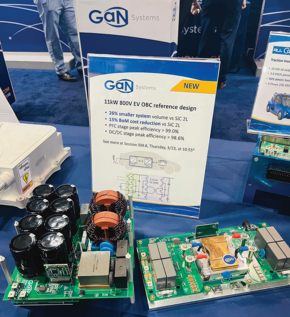
A 11 kW/800 V OBC design using GaN transistors has a 36% higher power density and up to 15% lower Bill of Materials (BoM) cost compared with a design using SiC devices.
This design combines a three-level, flying capacitor topology for a bridgeless, totem-pole PFC structure and dual active bridge in a three-level topology. This three-level design reduces the transistor voltage stress by half and allows the economical, 650 V GaN to be used in this and many other 800 V applications.
Gate drivers
Some of the challenges of these systems include increasing power density to minimise the size of the OBC to meet higher power levels up to 22 kW. As battery voltages have risen from 400 V to 800 V, the industry has seen a wider adoption of SiC instead of the traditional IGBTs to increase efficiency and power density.
As battery voltage continues to rise, it is vital to have isolation in these systems to ensure safety with high bus voltages and high power levels. Several isolation approaches can be used in OBCs and offer up to 5 kV RMS isolation.
Isolated gate drivers
Dual-channel, automotive-grade, isolated gate drivers have varying package options that can achieve up to 5 kV RMS isolation. They need their own power supply, typically up to a 4 A source and 8 A of sink current to enable higher efficiency, and to allow for the SiC or IGBT FETs to be turned on and off faster.
The isolated drivers have both a wide-body (WB) SOIC-16 package and an SOIC-14 WB package that offers 3.3 mm creepage between the output drivers. The SOIC-14 WB package is recommended for 400 V/800 V systems as it boosts creepage between the high- and low-side outputs.
Power supply
An automotive-grade LLC transformer driver can be used for the isolated, biased supplies. This device can work with SiC MOSFETs as an isolated bias for SiC gate drivers.
A flyback topology is often used for isolated power supplies to provide an isolated, 18 V/-4 V output that drives the SiC FET with a 18 V/-4 V output. The number of outputs can be configured based on the transformer, and the output voltage (VOUT) can be altered via the turns ratio.
An LLC converter is the most efficient topology for the isolated power supply for the gate driver. It uses a resonant LLC tank, which has a magnetising inductor for energy transfer, as well as an additional capacitor and inductor that make the tank resonate at a certain frequency.
The converter uses this resonance to achieve soft-switching and ensure highly efficient power conversion.
The main benefit of LLC converters is that the leakage inductance created by the transformer can be used as the resonant inductor in the tank. This eliminates the voltage spike induced by the leakage inductance and improves efficiency, compared with flyback topologies.
This soft- switching topology also helps when considering electromagnetic interference since there is no overshoot or ringing, which is common with a hard-switching topology such as a flyback.
The LLC resonant topology offers several notable advantages when compared with a half-bridge driver. A half-bridge driver requires a microcontroller, as well as two external FETs, which can lead to a larger-sized solution and more complex design.
Devices integrate the half-bridge driver with a controller and FETs in a 2 mm x 2.5 mm package, which reduces not only the total cost but also the number of components that must be sourced, as well as manufacturing complexity. This includes protection features such as over-current protection (OCP), over-temperature protection (OTP) and soft-start.
LLC isolated bias supply vs flyback
Another common topology used for the gate-driver bias supply is the primary-side regulation (PSR) flyback topology. One advantage of an LLC resonant topology is its reduced solution size, due to the switching frequency (fSW), which can reach up to 5 MHz.
Meanwhile, flyback topologies have an fSW below 400 kHz. This results in a total solution size that can offer a similar power level while being 40% smaller.
High-frequency LLC power supplies are typically more difficult to implement and optimise in designs than low-frequency converters. However, integrated devices simplify the LLC power-supply design with features such as automatic resonant frequency detection, integrated FETs and an integrated controller.
In addition, LLC resonant topologies reduce the size of the gate-driver power supply, increasing the power density for high-power OBC designs.
Conclusion
GaN transistors are an increasing focus for driving the smaller size and higher efficiency of OBC designs.
While silicon can be lower cost, and SiC can offer higher performance and efficiency, GaN can provide both and smaller size, even when using a three-stage front end.
This is creating more opportunities for integrating the OBC with the
DC-DC converter, and even the inverter. This allows the three elements to share cooling – usually liquid – in a smaller space, leaving more room for the battery pack.
Acknowledgements
The author would like to thank the following for their help with this feature: Wayne Liang at Microchip and Rafael Garcia at Infineon Technologies.
Some suppliers of onboard chargers
Bel Power
BorgWarner
Ennovation Technology
IES Synergy
Infineon
Microchip Technology
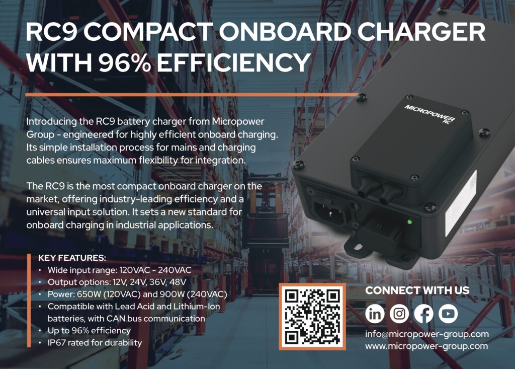
Micropower Group
Monolithic Power Systems
NetPower
Texas Instruments
Vitesco Technologies
Wolfspeed
Xepics
Yageo
+1 201 432 0463
+1 248 754 9200
+48 885 806 086
+33 4 99 13 62 80
+49 89 234 65555
+1 480 792 7200
+46 470 72 74 00
+1 425 296 9956
+1 972 560 0500
+1 972 9953773
+49 9132 82 0
+1 919 313 5300
+39 075 969 6472
+886 2 6629 9999
ONLINE PARTNERS


