Isolation technologies
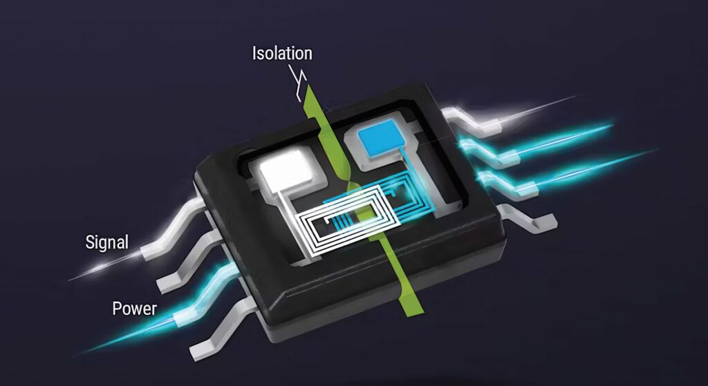
(Image courtesy of Texas Instruments)
Isolated states
Nick Flaherty investigates techniques that enable digital controllers to interface safely with high-voltage systems
As automotive designs move to electrification, high-power electronics have become critical components in new electronic drivetrain and battery systems. Communication and control from low-voltage digital devices requires electrical isolation of the high-voltage elements from the low-voltage side, covered by the extra-low voltage (SELV) regulations. This allows for existing 12 V power, 24 V in offroad vehicles and emerging 48 V designs.
In all these applications, galvanic isolation, usually semiconductor-based, is required to allow digital controllers to interface safely with the high-voltage systems of a modern EV.
A typical EV combines many power functions, including the traction inverter, climate control and heating, and the onboard charger. These systems operate at radically different voltage levels that must be isolated.
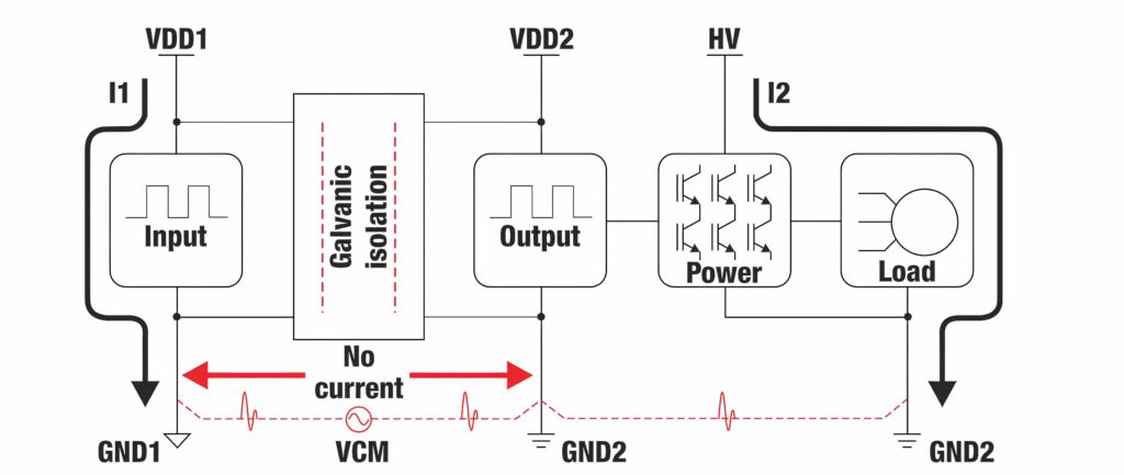
Galvanic isolation prevents the flow of current between the different voltage domains while still supporting the flow of data and power, and it can be integrated into a power device such as a gate driver that controls the inverter.
Other approaches, such as optical isolation and electromechanical contactors, can cut off the high-voltage portions of a vehicle to protect both the equipment and the users. Electromechanical contactors are particularly vital for offroad and industrial vehicles, such as agricultural equipment and electric mining trucks with huge battery packs delivering large amounts of power.
Historically, galvanic isolation for data transmission has been implemented using optical technology, with an LED or laser source and a photodiode receiver. However, the demands of the automotive market in general, and EVs in particular, have spurred the development and adoption of digital isolation technologies to offer an alternative.
Fundamentally, the first priority in any high-voltage power system is to protect maintenance personnel, operators, drivers and passengers. Galvanic isolation satisfies this priority by isolating the high voltage from other low-voltage human interface sections.
The second priority is to establish reliable, safe operation between high- and low-voltage circuits, such as voltage and current sensing, power-supply control, digital communications and signal processing. Reliable isolation techniques, materials and controllers allow designers to satisfy this priority.
This means isolation needs to cover voltage, current and communication signals, and it needs to assure safe and useful battery voltage.
Current isolation protects batteries from overload or high charging rates with an isolated current sensor that monitors the discharge and charge currents. Digital isolators enable safe and robust data communications for the CAN or serial bus. This can be galvanic or optical isolation, and there are design tradeoffs for both.
High-voltage systems require additional isolation because more bi-directional signal information is communicated across the isolation barrier. Many analogue and digital circuits have specific bias voltage requirements, where both digital signals and power cross the barrier.
An isolated, high-resolution, analogue-to-digital converter (ADC) may require 3.3 V in the same system, whereas an isolated gate driver may require +15 V and -5 V. These requirements necessitate not just the transfer of signals across the isolation barrier, but power as well.
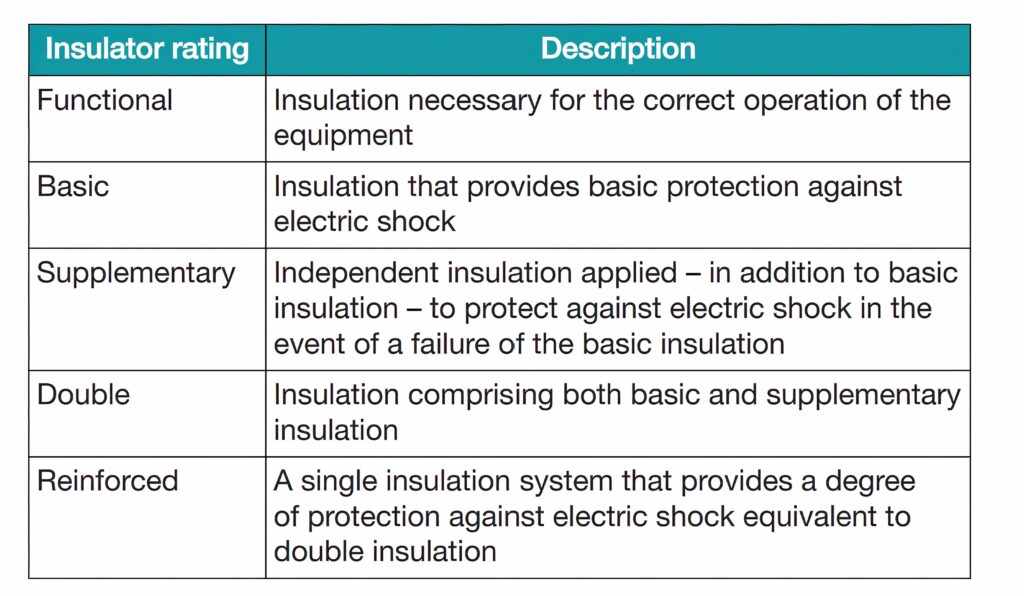
(Image courtesy of Texas Instruments)
Types of isolation
There are three main types of galvanic isolation: functional, basic and reinforced.
Functional isolation refers to the minimum amount of isolation assigned to a system so that it will function properly without necessarily protecting against electrical shock. One example is proper printed circuit-board (PCB) conductor spacing for a given voltage rating.
Basic isolation provides sufficient protection against electrical shock, with a safety rating on a parity with the highest system-level voltage. This is only intended to provide a single level of protection against electrical shock and it cannot be considered fail-safe. While these devices are accessible to a user, they must be contained within the system. Basic isolation devices are 100% safety tested at 2.5 kVac RMS for a period of one minute and typically have a minimum creepage of 3.2 mm.
Reinforced isolation is the highest commercial rating applied to high-voltage systems. One way to meet requirements is to introduce further distance across the isolation barrier such that it can withstand higher-voltage testing standards and a longer rated lifetime. This provides two levels of protection, making these devices fail-safe and allowing user access. They are 100% safety tested at 5 kVac RMS for a period of one minute and typically provide a minimum creepage of 6.4 mm.
Isolators have several important parameters regardless of the technology used. The creepage and clearance distance, for example, is the shortest distance between two conductive leads across the isolation barrier.
The creepage distance is the shortest distance measured between adjacent conductors across the surface of an IC package, whereas clearance distance is measured through the air.
Package technology plays an important role in achieving higher measures of creepage and clearance distance by providing various options for engineers. High-quality mould compounds, wide-body packages and higher reinforced isolation ratings must complement each other, so the packs don’t break down and arc, says Tim Merkin, senior member of the technical staff at the Kilby Labs of Texas Instruments (TI).
Another parameter is current-mode transient immunity (CMTI), which indicates an isolator’s ability to operate reliably in the presence of high-speed transients and it is measured in kilovolts per microsecond or volts per nanosecond. The proliferation of wide-bandgap semiconductors, such as silicon carbide (SiC) in inverter and DC-DC converter designs, has resulted in higher transient-voltage (dV/dt) edge rates, making the measure of CMTI critical for gauging an isolator’s resilience.
High-performance isolators have CMTI ratings that easily reach 100 V/ns, and many are tested in excess of 200 V/ns. A low CMTI isolator operating in a high dV/dt environment can expect to have signal integrity problems, such as pulse jitter, distortion, erratic operation or missing pulse information.
Isolation trade-offs are similar at IC and system level. Smaller IC package sizes, higher integration, thermal management and compliance with certification standards often compete against the need to reduce EMI and achieve higher efficiency. Selecting isolated components that are designed to meet all of these needs at IC level helps to facilitate a seamless transition to fully reinforced compliance at system level.
(Image courtesy of Texas Instruments)
Battery management system
The need for current isolation is highlighted by a distributed BMS with multiple packs of cells, each with a remote BMS control unit. In this configuration, measurements on cells within the battery modules are made by the remote BMS units and reported over a series connection to the BMS master controller. Current measurement for the full stack is made using a shunt resistor at the bottom of the stack and an isolated current amplifier.
The BMS controller can calculate the voltage of the full stack by adding the voltages of the modules, but a redundant safety-check, isolated-voltage measurement of the full stack can be made using a resistor divider and isolated-voltage sense amp, such as the Si893x.
The entire system can be monitored and controlled via an automotive bus, such as CAN, which is isolated with a digital isolator.
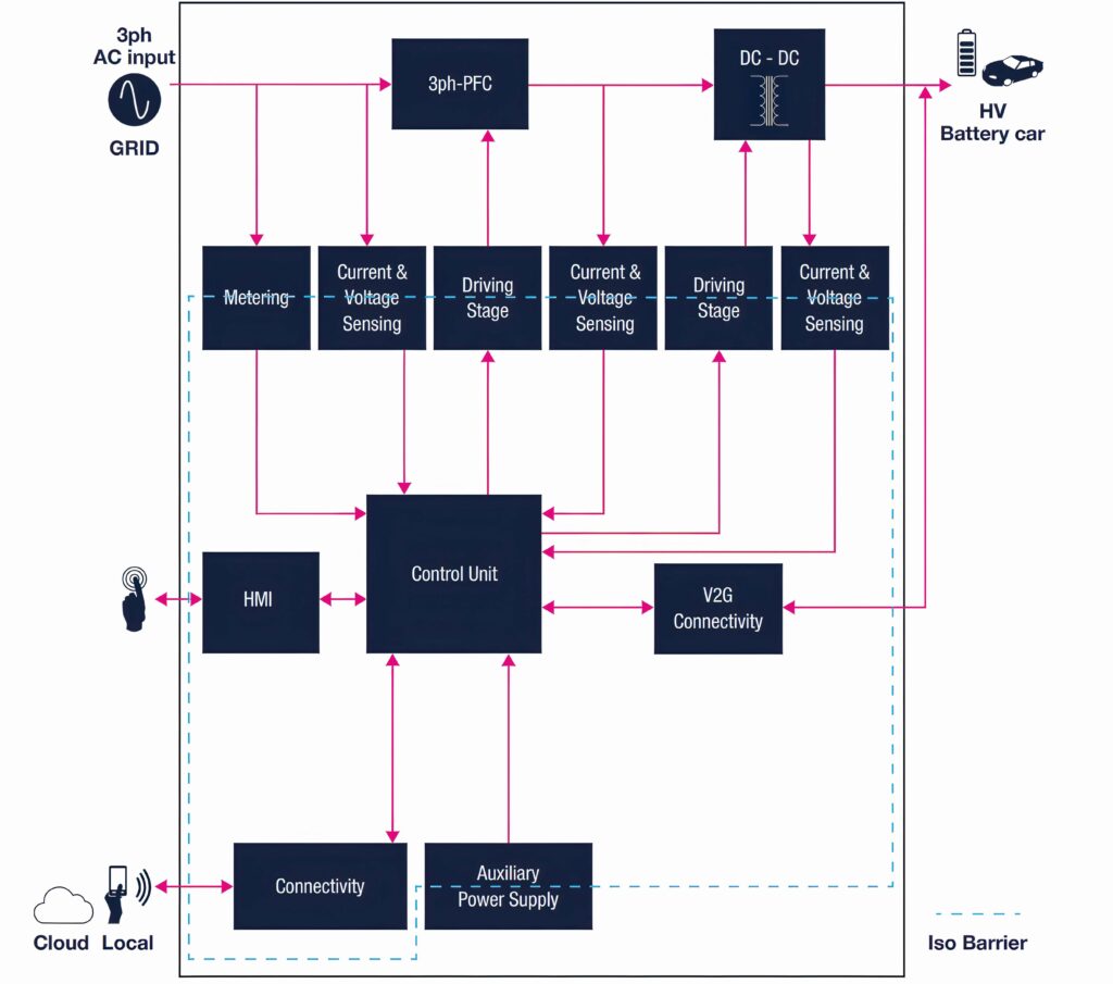
(Image courtesy of STMicroelectronics)
Gate driver
The gate driver is a common example of galvanic isolation, separating the control signals sent to high-power transistors from the high voltage. This isolation can be handled by layers of silicon oxide in the chip or by coupled wires in a package.
Innovations in the isolated gate driver can help vehicle performance. By varying the gate-drive strength in steps between 20 A and 5 A in real time, designers can improve system efficiency with a gate driver by as much as 2% by minimising SiC switching power losses. This can result in up to seven more miles of EV driving range per battery charge. For an EV user who charges their vehicle three times per week, that could mean more than 1,000 additional miles per year.
The isolated SPI programmability, and integrated monitoring and protection features in a device such as the UCC5880-Q1 from TI can reduce design complexity, as well as external component costs. Engineers can further reduce components and quickly prototype a more efficient traction inverter system using a reference design with SiC high-voltage transistors. This customisable, tested design includes the UCC5880-Q1, a bias-supply power module, real-time control MCUs and high-precision sensing.
“Designers of high-voltage applications like traction inverters face a unique set of challenges to optimise system efficiency and reliability in a small space,” says Wenjia Liu, product line manager for high-power drivers at TI.
“Not only does this new, isolated gate driver help enable engineers to maximise driving range, but it also integrates safety features to reduce external components and design complexity. It can be easily paired with other high-voltage power-conversion products, such as our UCC14141-Q1 isolated bias supply module, to improve power density and help engineers reach the highest levels of traction inverter performance.”
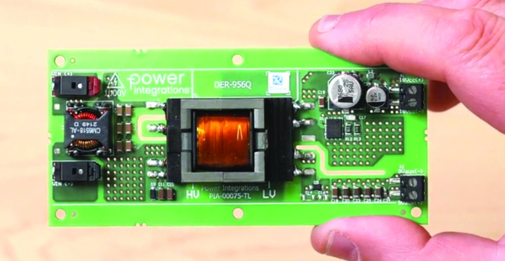
(Image courtesy of Power Integrations)
Inductive isolation
The development of hybrid and EVs means the voltage range for batteries has risen to 400 V or even 800 V. Devices with an integrated, high-voltage switch and internal isolation enable compact power-supply design for these new vehicles, and provide significant benefits.
Inductive isolation within the package eliminates the need for an optocoupler (also known as optical isolators) as there is a high-voltage switch, a primary side controller and a secondary side controller.
The isolation greatly reduces component count and increases performance uniformity across production. These benefits simplify design and can increase reliability. With the move to high-voltage systems, ensuring an electrical fault will not cause shock, harm or injury to the end-user is critical.
Power Integrations has developed a method of evaluating package safety isolation, where an artificially induced catastrophic failure of the power switch is used to cause package damage in the vicinity of the high-voltage switch. Post-failure isolation tests demonstrate that the integrity of the isolation barrier within the semiconductor device is maintained, says Thomas Anthony Capobianco at Power Integrations.
Safety standards apply to both system designs and integrated circuits. Specific standards are also used for qualifying automotive products.
The UL Standard for Safety for Optical Isolators, UL 1577, covers optocouplers and photocouplers. Aside from these, it also applies to non-optical devices that perform similar functions in terms of isolation and signal control.
The FluxLink technology developed by PI uses magneto-inductive coupling, where an isolation transformer forms the lead frame of the IC to provide internal isolation.
Section 11 of the UL standard defines an important dielectric voltage-withstand test that is used to determine whether a device is capable of withstanding a potential surge equal to the rated dielectric voltage for 60 s without breakdown. This is commonly known as the High Potential (HiPot) test.
The IEC 60747-17 standard covers magnetic and capacitive coupling for isolation, and it uses a test voltage that can be a transient, repetitive or continuous voltage under specified conditions. Passing criteria state that no external or internal flashover occurs during testing.
For example, in the InnoSwitch3-EP, a 1700 V, high-voltage switch, driver, primary and secondary controller is combined with protection circuitry. Secondary-side regulation is achieved using the proprietary feedback mechanism for the control loop. This internal isolation eliminates the need for an optocoupler, which reduces component count and increases system reliability, but means that the InnoSwitch3-EP requires package safety isolation testing.
The goal of this qualification was to demonstrate safety, not only during normal operation but also in the event of a catastrophic failure.
Regardless of implementation, isolators must meet safety standards for robust galvanic isolation. They must also be reliable enough to outlast the equipment they are installed in, which, in the industrial world, can mean decades of use. Designers must ensure isolation circuits can withstand electrical stresses that can cause physical damage and reject data-corrupting noise from any number of sources.
Therefore, the designer must carefully consider key isolator operating parameters, such as common-mode transient immunity, key timing parameters, such as propagation delay and pulse-width distortion and field-related specifications, such as EMI and RF susceptibility.
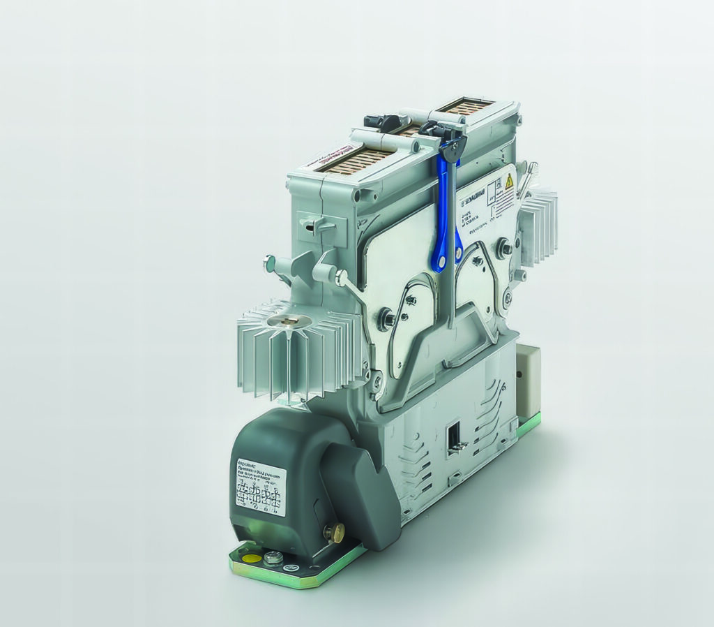
(Image courtesy of Schaltbau)
High-voltage insulation
Insulation reliability directly affects the isolator’s ability to safeguard against user exposure to high voltage and it is of paramount importance. The insulator is the heart of the isolation barrier and key to maintaining system safety. It is very important that the insulation be uniform without voids, which can cause a localised breakdown.
Insulator uniformity is a function of the insulator material and the fabrication process. The dielectric strength of the optocoupler’s injection-molded plastic compound can vary by as much as 300% due to voids created during fabrication.
In contrast, the CMOS digital isolator uses semiconductor oxide layers for its primary insulator. The CMOS oxide deposition process is tightly controlled and highly uniform, and the resulting variation in dielectric strength is only 20%. Each oxide layer has a breakdown voltage of 500 Vac RMS per micron.
Higher voltages (such as 5 kVac RMS) are implemented by simply stacking oxide layers during wafer fabrication. The result is a higher absolute maximum breakdown voltage in a substantially smaller size than optocouplers, and insulator reliability that is independent of the packaging process.
Optocouplers require current to bias the LED and some form of bias on the output side. The total input plus output current varies widely, depending on the type of optocoupler. When forward-biased, the optocoupler LED is low-impedance, and device power consumption increases with LED forward current, which can range from 1 mA to over 15 mA. In some cases, the LED may require an external driver, further decreasing system efficiency, while increasing BOM complexity and cost.
The optocoupler output impedance can be low or high, depending on its architecture. High-speed optocouplers have an active photocoupler and output driver that requires an external bias voltage. Such devices have low output impedance, but at the expense of increased total operating current, which can range from 15 mA to over 40 mA.
Compared with optocouplers, CMOS digital isolators offer significantly higher operating efficiency, consuming about 1.7 mA per channel at 10 Mbps at VDD = 5.0 V with a 15 PF (power factor) load. Its high-impedance input buffer consumes only microamps of leakage current, while its 50 W CMOS output driver can source or sink 4 mA.
The bulk of the CMOS digital isolator’s power savings results from the use of an RF carrier instead of light, eliminating the power-hungry LED. Losses in the isolation path are minimised by the isolation capacitor structures, which are optimised for robust data transfer and minimum power loss. The CMOS digital isolator’s power dissipation remains relatively flat and substantially less than that of the optocoupler.
Integration challenges
New power-conversion architectures can create issues for isolation. The integration of the onboard battery charger with the traction drive reduces the overall size and complexity of the system, but can present safety issues due to the absence of an isolation stage.
Most carmakers require an isolation stage galvanically separating the grid from the battery, but this is not provided by most integrated chargers. Additionally, some designs produce torque at the shaft during charging, which may cause vibration and the need for rotor locking.
Some designs even require free-shaft continuous rotation of the rotor during charging at grid electrical frequency, complicating the mechanical arrangement, and introducing relevant friction and ventilation losses during charging. They are also unidirectional, so do not allow vehicle-to-grid (V2G) operation.
To address these issues, researchers at the University of Torina, Italy, have integrated the onboard battery charger with the traction drive of road EVs equipped with a six-phase, traction motor drive. They developed a charger that is deeply integrated within the e-drive powertrain to reduce the cost and volume of the e-axle with respect to non-integrated solutions, but still providing galvanic insulation.
Dedicated control strategies are developed and tested for regulating the AC grid current at unitary power factor and low total harmonic distortion (THD), and to avoid torque production or rotor movement during charging independently of the rotor position. Extensive simulation results show the feasibility of the proposed solution, together with a proof-of-concept validation on a commercial traction motor.
Multi-phase designs are increasingly popular, permitting a reduced phase-current rating and higher system reliability. Torque-ripple mitigation, a higher number of degrees of freedom for the control and better thermal management are also additional benefits. In particular, the adoption of six-phase motors appears to be the best trade-off between the benefits of multi-phase machines and increased system complexity, permitting a relatively easy transition from the traditional three-phase drives.
The Isolated Fully Integrated OBC (IFI-OBC) concept developed by the researchers adds a control strategy that requires a dedicated transformation matrix for defining the inverter reference voltage.
This integrated OBC enables accurate control of grid current quality and the absence of motor torque during charging. Finally, differently from many other topologies, the proposed OBC is bi-directional, permitting V2G operation. The design has been validated by accurate simulation models and experimental tests on a proof-of-concept test rig using a commercial, 96 kW traction motor.
The isolated onboard battery charger has been developed and integrated with a traction motor drive, based on a six-phase permanent magnet synchronous machine (PMSM).
The topology implements galvanic isolation between the grid and the battery by exploiting the traction motor as a transformer, without the addition of electrical hardware out of the drive itself, except for a reconfiguration selector, which may be electrical or mechanical, depending on the specifications of the carmaker.
Electromechanical isolation
With traction inverters, battery packs and charging systems operating at ever higher voltages, 1500 V contactors are being used to protect a vehicle and its users in the event of a short-circuit or accident. These are electromechanical relays that stay connected until there is a problem, when they open to cut the circuit.
These are used in the battery disconnect unit (BDU) for all varieties of electric platform, from passenger vehicles to offroad and agricultural equipment and electric shipping, where there are high-power battery packs, as well as the associated charging systems.
“Initially, we came from developing rail systems, and we have 3000 V and 2000 A, but this is too big for automotive, so now the learning curve has taken us to 1500 V and 350 A,” says Pavel Tomashev, product manager, contactors at Schaltbau.
One of the key challenges with a contactor is arcing when the contacts open. This requires a fast response to prevent the arcing from welding the contacts shut.
“That means we know how to handle the arc reliably and we know a lot about efficiency with the lowest possible contact resistance. The main body is made from copper, but the contact points have silver tin-oxide tips that are welded to the contactor body, and it has a much higher stability and oxide stability over time.”
That’s where the controller board, called the economiser, provides the pull to keep the contactor connected in a process that takes less than 100 ms.
“What is also important is that we have a current sensor and temperature sensor alongside the voltage sensors, so that contact pressure remains stable. To avoid the contact pressure drop from current change, we do the temperature correction and adjust the current,” Tomashev adds.
“Arcing is always there to break the current flow. Welding is another type of problem. You can see welding at the startup with a high in-rush current from the capacitor on the inverter, and the contactor has to survive that process. Pre-charge circuits are widely used, but if the pre-charge doesn’t work, the contactor still needs to open.
“The silver tin oxide has a higher melting point, so it is more resistant to the welding, and we use a coil drive that reduces the contact bounce. As long as you make the contact quickly without bouncing, [this] is the way to make the contact. On the mechanical side, contact springs prevent bounce, which keeps the contacts closed.
“The contact is not fixed on the armature. There is a certain level of freedom to get overtravel and this is crucial to avoid contact bounce. There is a powerful spring with a flexible connection between the armature and the contact to prevent the contact from bouncing,” he adds.
High-power contactors used for renewable energy systems such as wind turbines are often filled with an inert gas, but for e-mobility applications, including electric ships, there is an advantage to having contactors that are open to the atmosphere, Tomashev says.
“They are open-air insulation, so there is no special gas, no hydrogen, no vacuum,” he explains. “What is important in a failure case with a short-circuit current of 5-10 kA is huge energy that generates an electromagnetic force that pushes the contact back, opening the contact. We call it levitation during the short-circuit.
“We handle that in a similar way with a high melting-point material, and there is no risk of explosion with open air, as the high current creates a lot of extra pressure, heating the air to a temperature of 1000 C for milliseconds.
“That is a problem for sealed contactors that cannot let the pressure out. That’s what helps us contribute to electrical isolation, even in the case of a short-circuit, to open the main contact circuit to ensure proper isolation, based on our experience with contactors in rail systems installed under the railcar body. With all the humidity, dirt and snow, over decades we have seen no issues with that.”
These contactors provide safety and efficiency, in that there is less risk of welding and no risk of explosion, and they use an efficient coil drive and main circuit.
“Our calculations on charging station applications and general operation profile show contactors with a resistance of 100 µΩ versus the industry average of 200 µΩ can save more than the price of the contactor in less than a year, and the efficiency boosts the performance of the chargers or the battery packs,” says Tomashev.
At the heart of isolation design for e-mobility is the safety of the people and the equipment. As more systems become electrified with ever-higher power levels, isolation technologies will play an ever-greater role. In a variety of ways, these are responding to the need for more efficiency, safer systems and new architectures.
Click here to read the latest issue of E-Mobility Engineering.
ONLINE PARTNERS


