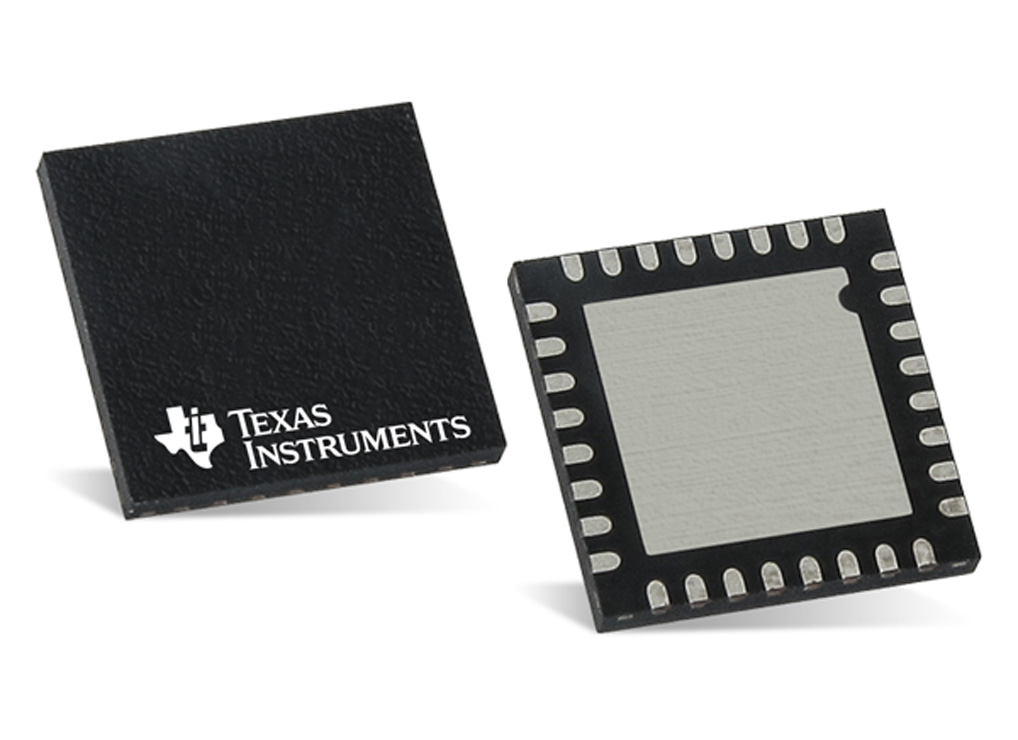
GaN switch at 650 V ‘sweet spot’

Texas Instruments (TI) has produced a 650 V gallium nitride (GaN) power switch for EV designs (writes Nick Flaherty).
It is combined with a silicon gate driver in a single package to simplify the design and management of power systems. The combination has been under test with customers for the past two years, gathering 40 million hours of reliability data before the launch.
Using GaN at a switching frequency of 2.2 MHz, rather than the 150 kHz for silicon MOSFET power switches, provides 99% conversion efficiency. The higher frequency also reduces the size of the magnetics by 56%, in turn reducing the size and weight of onboard chargers and inverters.
An on-resistance of 30 mΩ reduces the thermal losses and the size of the heat sink required. Top- and bottom cooled variants of the 12 x 12 mm package are available.
“For every 1 W you save in efficiency you can save 1 W in cooling, so you get a magnifying effect in reducing losses, and you can charge faster,” said Steve Lambouses at TI.
The company says 650 V is the sweet spot for EVs up to 54 kW, and doesn’t plan to support higher voltages. Higher voltage designs can be supported with the switches in parallel, synchronised by the controllers.
The silicon driver supports an ideal diode mode for the GaN switch. This allows optimisation of the dead time in a switching topology for higher efficiency, as the GaN FET is turned on automatically by the built-in gate driver after a very short delay when a negative drain to source voltage is sensed.
ONLINE PARTNERS


